| English | Japanese |
|
|
Yesterdays access |
| Page Top | [Lily Diary.】 A diary of life in Mindanao. |
| 26/03/17 | How to establish a radio club in the Philippines |
| 26/03/10 | Using KENWOOD AT-300 with YAESU radio |
| 26/02/27 | Philippine NTC Amateur Radio License Examination Question Bank |
| 26/02/20 | Package received from JK1SNS |
| 26/02/18 | Temporary License Renewal |
| 26/02/14 | Satellite Tracking Software SatTrack |
| 26/02/05 | Making a Repeater Controller Pert2 |
| 26/02/02 | CQ on satellite IO-86 |
| 26/01/27 | Shack & Repeater Controller |
| 26/01/16 | Making a Repeater Controller |
| 26/01/16 | Making aRotator Interface PCB |
| 26/01/10 | Satellite antenna installation |
| 26/01/08 | WSJT-X Remote Operation |
| 26/01/07 | JTDX Remote Operation |
| 26/01/04 | log_reciver_Ver2.6.6 |
| 26/01/04 | Tailscale VPN software for JTDX_Remote |
| Antenna Rotator Interface PCB Fabrication (2026/01/16) | ||
|---|---|---|
| At the 224th PRUG meeting (online), the topic of circuit diagrams and PCBs came up, so I decided to give KiCAD a try. I didn't know how to use KiCAD, so I was taught step by step by CatCPT, and in two days I was able to draw two circuit diagrams and turn them into patterns. 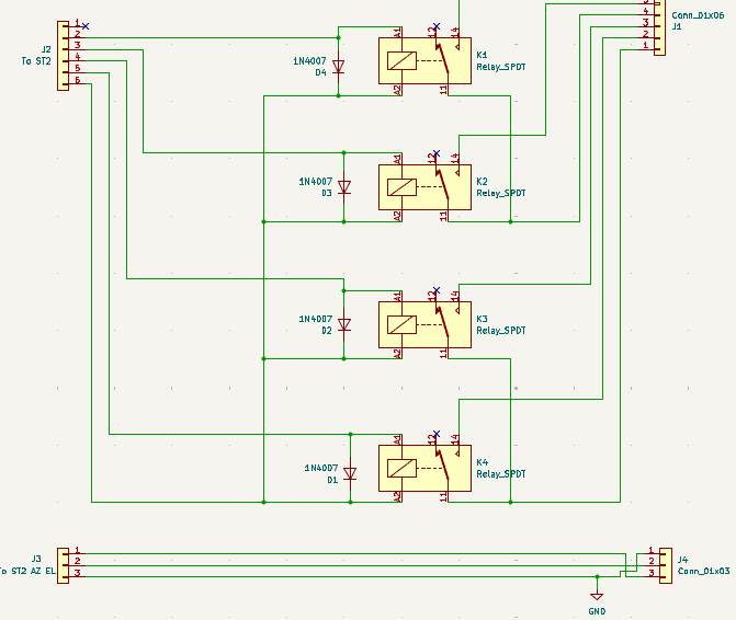 |
||
| It was made using this Janome board.Relay interface.I re-drawn the circuit diagram in KiCAD and created the board pattern. The relays are SRA-05VCD-CL, with four of them lined up. 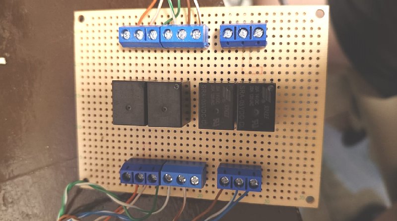 |
||
When wiring by hand, the patterns overlap.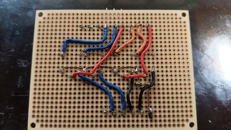 |
||
| At first I placed the relay next to it and then drew the pattern, but there were two places where the patterns intersected and I couldn't wire it. So I arranged the relays vertically and it was surprisingly easy to arrange the patterns. Even so, the process of drawing patterns from this circuit diagram is like playing a maze game and makes my head spin. As a 66-year-old, I think this work is good for preventing dementia. Once the pattern is created, run DRC on 'tool'-'Design Rule Checker' to check that there are no errors. Finally, create plot and drill files using 'file'-'manufacturing output'-'Carver' This is a Chinese circuit board manufacturerJLCPCB.I uploaded it to the website and got a quote, which was $2 for five 100mm x 100mm single-sided boards. 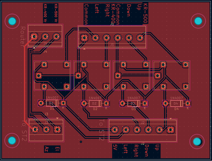 |
||
| January 10, 2026. January 16, 2026. |